
The probable drivers for quantum dot technology have been highlighted in a report from IDTechEx titled “Quantum Dot Materials and Technologies 2024-2034: Trends, Markets, Applications”.
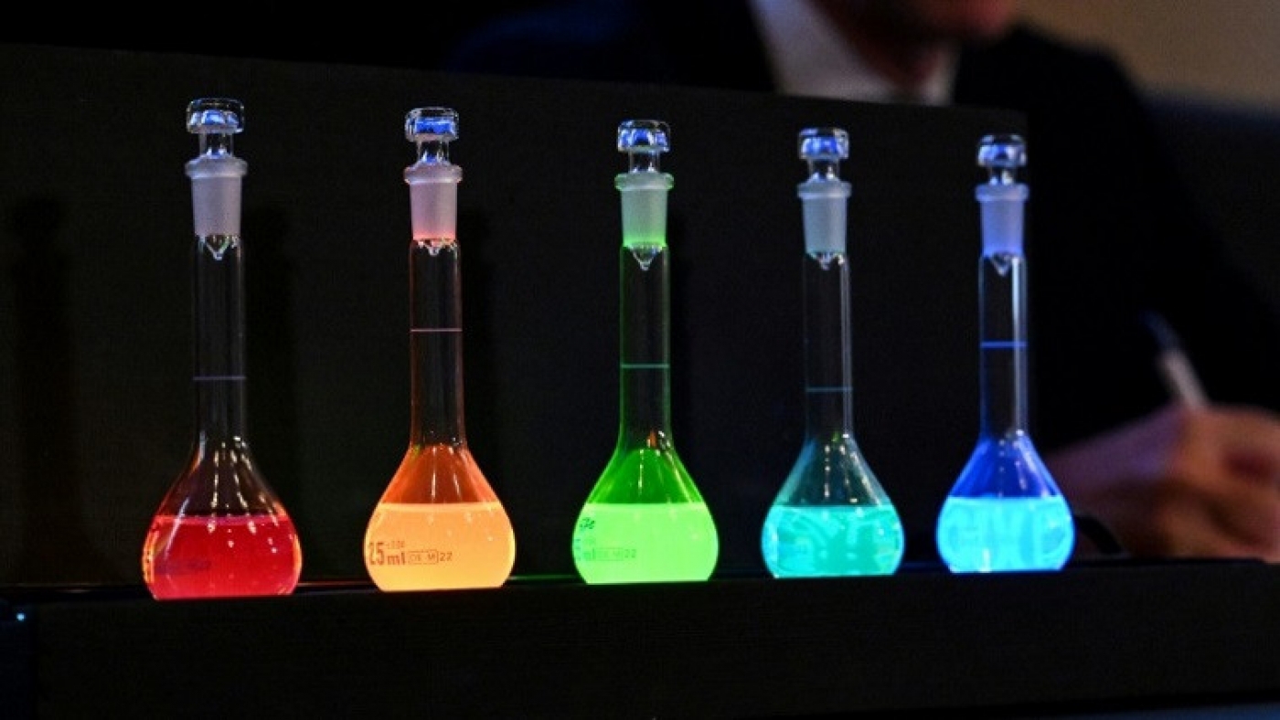
Quantum dots are tiny crystals that can be tuned to different colours. At one level this can provide greater clarity and image brightness to next-generation screens; at another level, the technology can improve medical imaging sensors.
Quantum dots were the subject of the 2023 Nobel Prize in Chemistry.
Quantum dots are semiconductor nanocrystals in the range of 2-10 nanometers (10-50 atoms) with size-tunable features. These structures exhibit quantum confinement effects as a property of their nanoscale dimensions.
Examples of ‘tunability’ include the control of quantum dots through photons that are used to excite semiconductor nanocrystals positioned in an array. The control of the photons forces an electron to move from its original place in the crystal lattice, leaving behind a hole. Illumination can also be controlled by virtue of an electron-hole pair being unable to revert to its energy ground state and therefore the light emission becomes suppressed.
The technology has special optical and electrical characteristics: photoluminescent and electroluminescent features. These quantum dot features can be adjusted by particle size, material, and composition.
This makes quantum suitable for use in dots displays, image sensors, photovoltaics, lighting, and various other applications. Here they capture and convert light into electronic signals that ultimately form images.
The most widely used material is silicon; however, for future technological growth, this has limitations for near-infrared and short-wave infrared. This can be partly overcome by using silicon Read-Out Integrated Circuit (ROIC) is still utilized although alternative semiconductors need to be identified for further advances with photodetectors. Examples include indium gallium arsenide and germanium.
Another candidate material is lead sulphide which offers the advantage of tunability across an extensive spectrum of wavelengths, enabling the sensing element can be arranged as a photodiode, photoconductor, or phototransistor.
Through this, it will be possible to create image sensors that can simultaneously achieve high resolution, low pixel pitch, and global shutter with potentially low costs.


 29
29 0
0  Printable